 Grzegorz "gsmok" Makarewicz,
The PCL86 tube belongs to the so-called "television tubes", i.e. tubes used in TV sets produced as the last models of tube televisions. In principle, the models produced at the end of the 70s and the beginning of the 80s of the last century are already transistor-tube constructions. A classic example of such a TV was "Libra" produced at the Warsaw Television Plant (WZT). I associate with this construction sentimental memories, because I belonged to the group of so-called "composers" who, as the name suggests, dealt with assembling these televisions from parts obtained from "Bomis" (younger Internet users need to search the web a bit to find out what it was).
Libra TV sets were owned by my neighbors and close family members. They were satisfied with the use of deficit devices at that time, and I had a nice financial source to support my modest student budget. With some embarrassment, I must admit that the television tubes used in "Libra" TVs were a necessary evil for me at that time. I had to accept this being dependent on the ideas of the designers of the WZT. Like other television set makers, I immediately gave them up as soon as full-transistor televisions appeared, such as Vela, Telefunken etc.
PCL86 tubes were really unlucky when it comes to their appreciation by audio equipment designers. The reason for this bad luck were ECL86 tubes, i.e. tubes with analogous parameters, but adapted to be heated with a voltage of 6.3V. For many years they constituted the basis for the construction of small low-frequency amplifiers. Their "TV equivalent", i.e. the PCL86 tube, was treated as a second-class tube not suitable for use in a tube audio amplifier.
Recently, after many years of "humiliation" PCL86 tubes are beginning to be noticed by the enthusiasts of tube sound. What is the reason for this? Could their mysterious sonic features be revealed? Nothing special. Simply, the inventories of ECL86 tubes have been practically exhausted and their prices have soared to very high levels. As a result, music listeners and designers have apologized to the previously unwanted "television product".
In the literature and publicly available online resources, you can find many schematic diagrams of low-frequency amplifiers based on the PCL86 (ECL86) tubes. The amplifier described here (in two versions) is based on the classic configuration recommended by the tube manufacturers. It is shown in Fig. 1. The schematic diagram shows one amplifier channel (right - R), the other channel is of course identical. Electronic components related to the left channel are marked with the letter "L" (e.g. C4L, R4L), components related to the right channel are marked with the letter R (e.g. C4R, R4R). Components common to both channels do not have an additional marking (e.g. C13, R13, LED1).
In addition, the schematic diagram included all the elements that allow you to build an amplifier in the version published in the journal Elektronika Praktyczna 2/2005. To assemble the amplifier in the form identical to that published in EP 2/2005, resistors R8L, R8R, R9L, R9R, R10L, R10R, R13, capacitors C10L and C10R and LED1 should be omitted, short-circuit the screen grids of tubess with a positive anode voltage power supply and use jumpers in place of the CLL and CLR chokes.

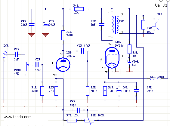
Fig. 1
Fig. 2 is a schematic diagram of the power supply system. It contains two power supplies. Tube filament power supply and power supplies generating anode voltage for both channels.
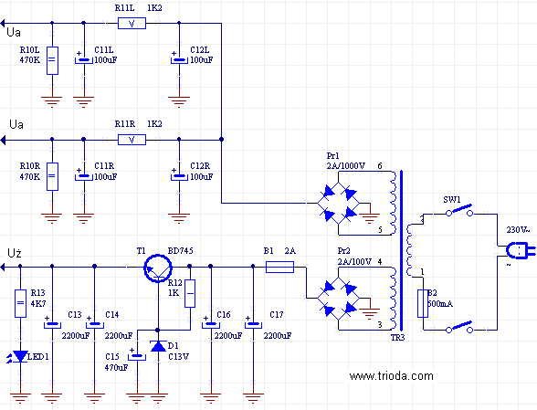

Fig. 2
I built the amplifier in two versions. They differ in mechanical construction. Both models are shown in Fig. 3.

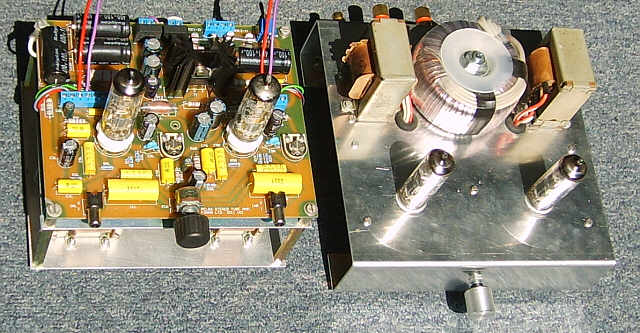
Fig. 3
On the left is the amplifier in the form of a "tower" and on the right is the amplifier made in the traditional form on a small aluminum chassis.
Amplifier version 1
The view of the amplifier in the form of a tower is shown in Fig. 4.

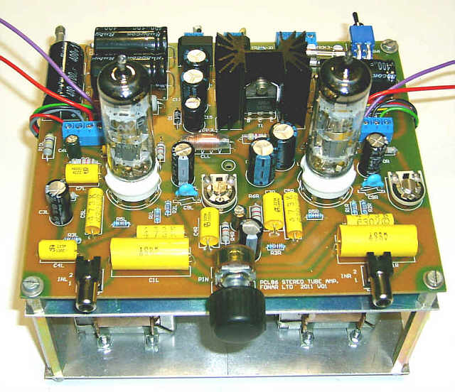
Fig. 4
For the first amplifier I designed a single circuit board shown in Fig. 5. As you can see, this is a single-sided circuit board that does not require any soldering jumpers.
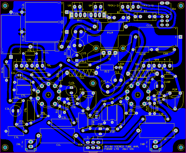

Fig. 5
Fig. 6 shows the outline of the components of the amplifier.
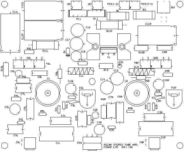

Fig. 6
The circuit board has been designed in such a way that it can be mounted not only electronic components, but also all additional components including input sockets, volume control potentiometer and power switch. Particular attention should be paid to the input sockets used so that they enable the correct connection of the signal and ground inputs. If necessary (no matching sockets), correct / swap the paths at the board entries.
Installation of additional components is of course optional. In the case of a housing that does not allow to insert a printed circuit board with these elements into it, sockets, a potentiometer and a switch should be mounted on the housing and connected to the board with wires. The view of the printed circuit board with mounted components is shown in Fig. 7.

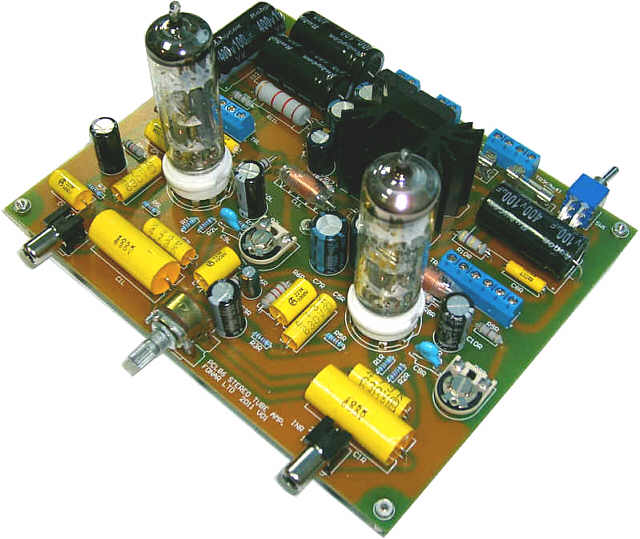
Fig. 7
On the printed circuit board there are descriptions and elements that match the markings on the schematic diagram. Before soldering the item, make sure that it has been installed in the right place. In this way, we will avoid having to desolder it - which is not a pleasure.
Installation is best started with the smallest elements (resistors R1L, R1R, R2L, R2R, R3L, R3R, R5L, R5R, R7L and R7R). Next, we mount the elements slightly larger (R4L, R4R, R8L, R8R, R12, R9L, R9R, R13, D1, R6L, R6R, R10L, R10R, C8L, C8R, B1, B2, CLL, CLR etc.).
In my experience, ARK connectors have a negative feature, which means that some leads can cause cold solder, so you should pay special attention to the soldering effect and it is best to clean them and do not touch them with your fingers before soldering.
Resistors R11L and R11R become very hot during amplifier operation. They should be soldered in such a way that they do not touch the printed circuit board. Make sure that the resistor R11L is as far away from the C12R electrolytic capacitor as possible. If this resistor is soldered on longer legs above the board, it may happen that during installation it will accidentally bend and come into contact with the C12R capacitor housing - this is unacceptable. This resistor should be bent as far as possible from this capacitor. If the design of the amplifier allows this, it is recommended to mount this resistor on the print side.
Heatsinks often have rivets mounted by the manufacturer to attach them to the circuit board. To mount this heat sink in a "traditional" way, these rivets must be removed and then the heat sink can be screwed on, e.g. using sheet metal screws (threading holes in the heat sink is not necessary). Make sure that the screw heads do not touch the tracks - this can happen when using screws with too large dimensions. Just in case, I recommend using insulating washers under the screws.
RCA input sockets are subjected to high stress when connecting or disconnecting cables. That is why the holes in the printed circuit board were designed in such a way that frequent wiring does not damage (break) the paths to which these sockets are soldered. Each socket, apart from the signal terminals, has two elements constituting additional mechanical stiffening. These elements have a square cross-section, and the diameters of the holes in the board are such that you need to use a significant clamping force so that the sockets are properly locked on the circuit board. If you have a problem inserting the socket, you can slightly round the splines with a file. It should be remembered that the more we file the fasteners, the easier it is to push the sockets, but the smaller their mechanical stability is.
The following drawings show the construction details of the amplifier assembled in the form of a "tower".

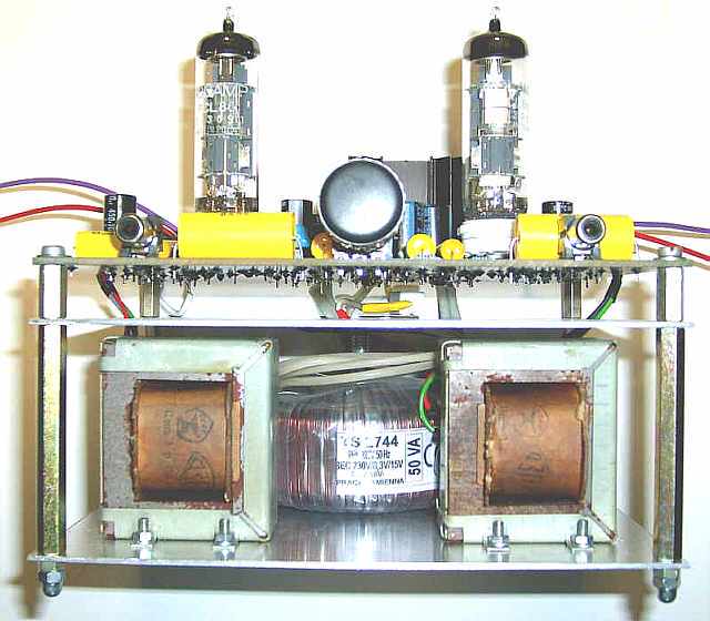
Fig. 8

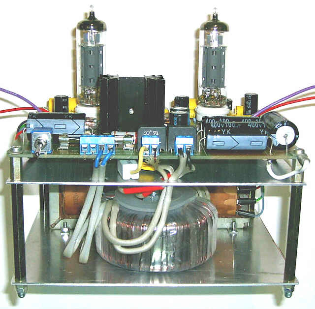
Fig. 9

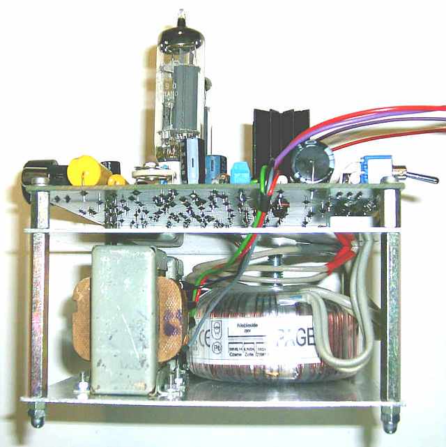
Fig. 10
Amplifier version 2
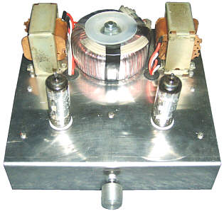
The view of the amplifier mounted on the aluminum chassis is shown in Fig. 11.

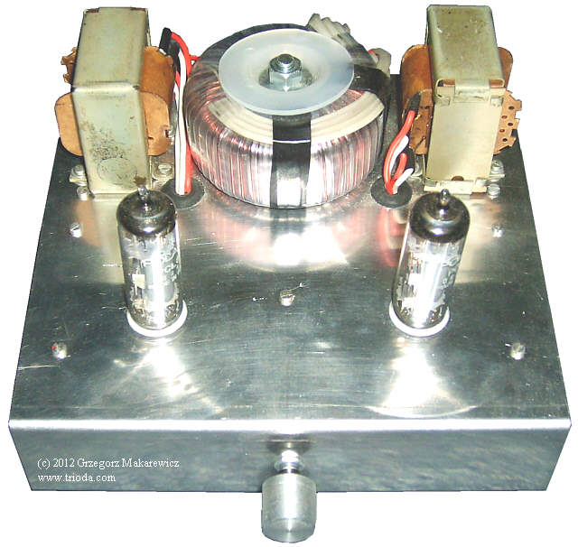
Fig. 11
The electrical system has been slightly changed compared to the first version. The schematic diagram of the amplifier is shown in Fig. 12.

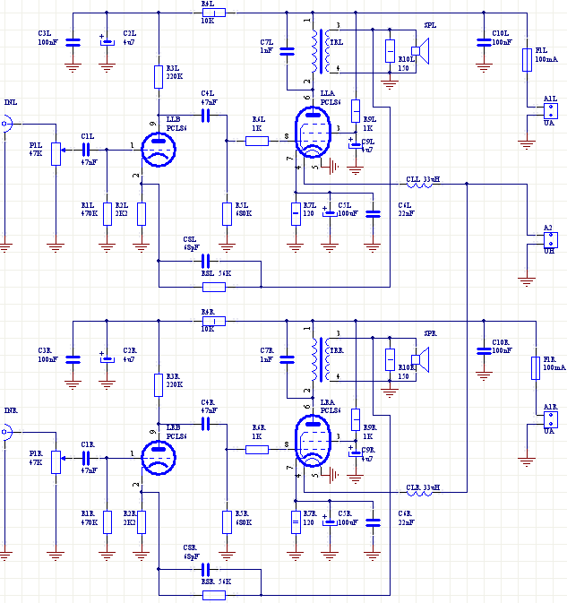
Fig. 12
The schematic diagram of the power supply is shown in Fig. 13.

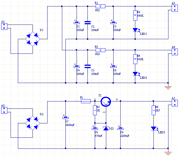
Fig. 13
The amplifier's components are mounted on two circuit boards. Fig. 14 and Fig. 15 show the view of the amplifier board and components from Fig. 12.

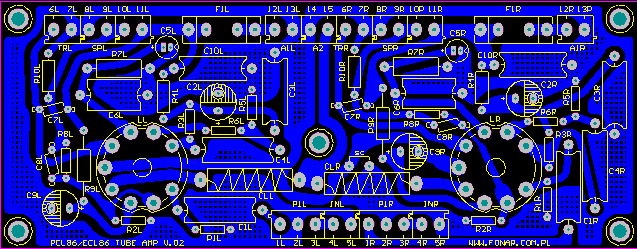
Fig. 14

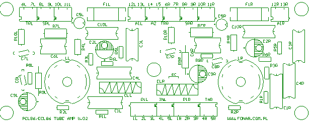
Fig. 15
Fig. 16 and 17 show the view of the printed circuit board and power supply elements from Fig. 13.

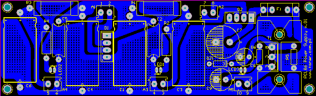
Fig. 16
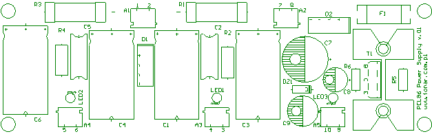

Fig. 17
Fig. 18 shows a photo of a partially assembled circuit board containing an amplifier section. There are no ARK connectors installed yet. As you can see the tube sockets and thus the electron tubes are located on the side of the printing paths.

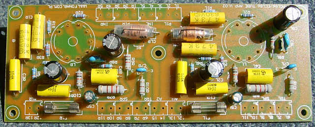
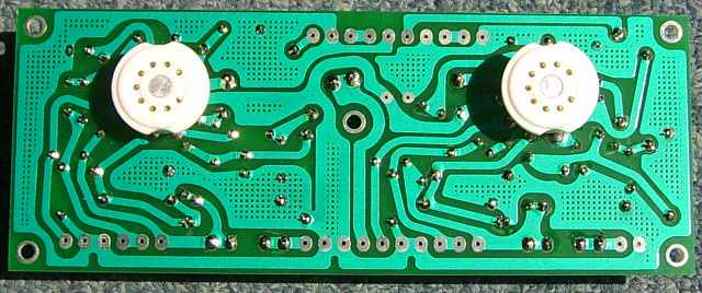

Fig. 18
In fig. 19 the printed circuit board of the amplifier power supply is shown. All components are soldered except for the transistor and the heat sink.

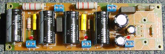
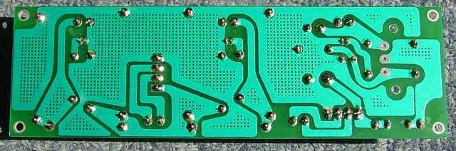

Fig. 19
The following figures show photographs of the structural details of the assembled amplifier.
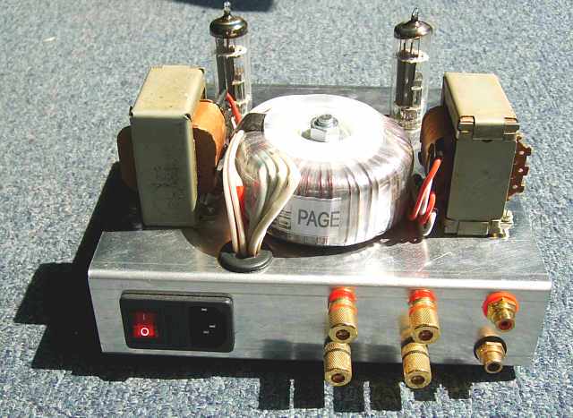

Fig. 20

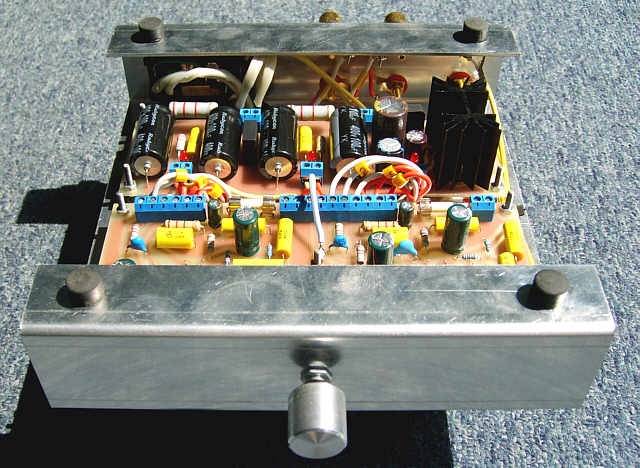
Fig. 21
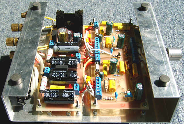

Fig. 22
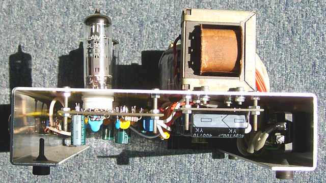

Fig. 23
Amplifier description published with permission from FonAr Sp. z o.o.
")
")
")
")
Comments powered by CComment